The Definitive Edition: Analysis of Every Single Intel Fab Across the US, Ireland, Israel, and Malaysia
The Lord of the Fabs and the Return of the King


(You don’t wanna know how long the face swaps took)
Intel operates logic and advanced packaging fabs across Arizona, Oregon, Ohio, New Mexico, Israel, Ireland, and Malaysia. I am going to cover the history of these fabs, the cleanroom sizes, and the process nodes.
Before we go into each fab, I want to cover the process node renaming by Intel. Intel led the industry for many decades and would often release a process node only for its competitors, such as TSMC and Samsung, to copy the name for their own nodes. This occurred even if the competitor node was vastly inferior. For example, Intel 10nm actually has the density and performance of TSMC 7nm.
This discrepancy led Pat Gelsinger to do a rename to make it easier to compare. So when you see Intel 10nm, think of the following comparison: Intel 10nm became Intel 7 which is equal to TSMC 7nm. When you see Intel 7nm, that became Intel 4. Now that Intel is trying to catch up to TSMC, they are doing a similar game since Intel 3 is not equal to TSMC N3E. Samsung has been cheating the whole time, so let us just ignore that.
If you want to see my WSPM model, skip to the end, but getting history and cleanroom sizes took forever. Please….
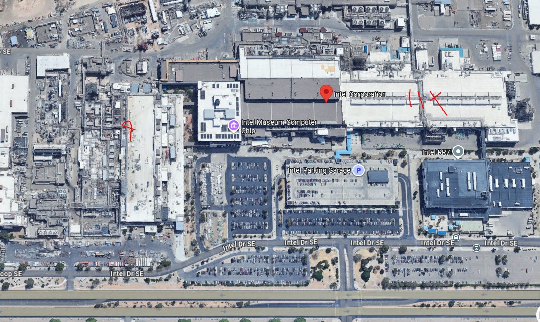
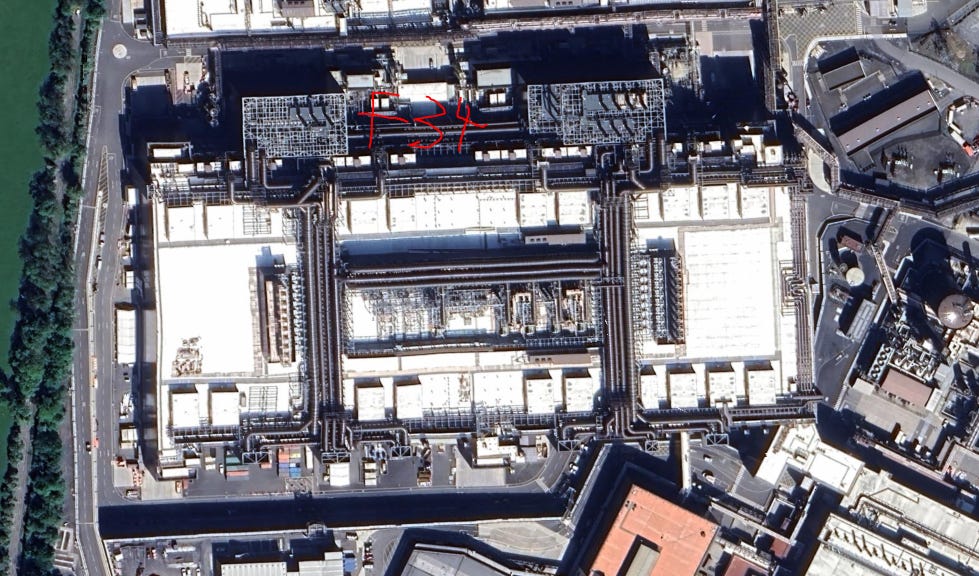
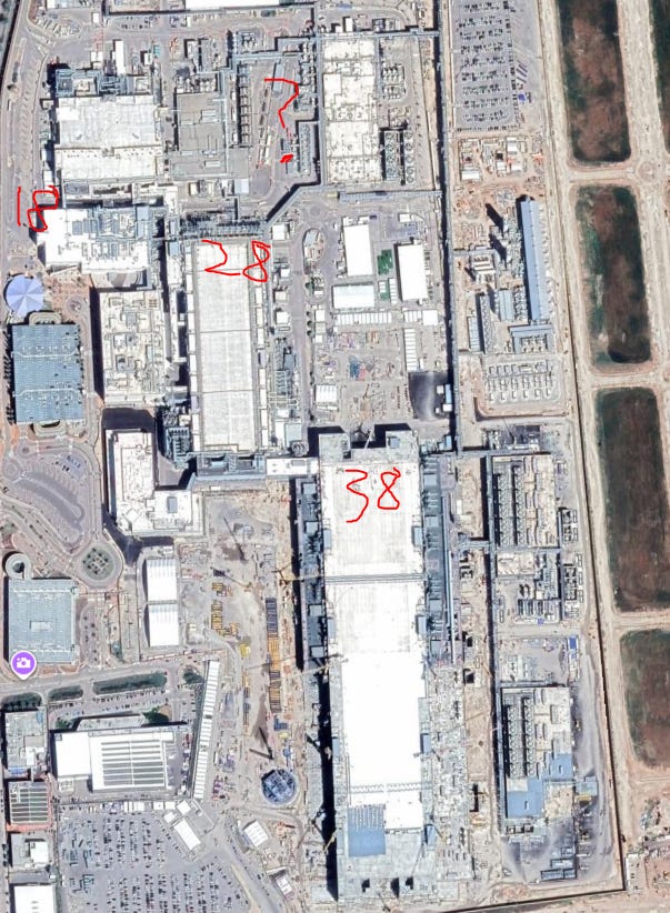
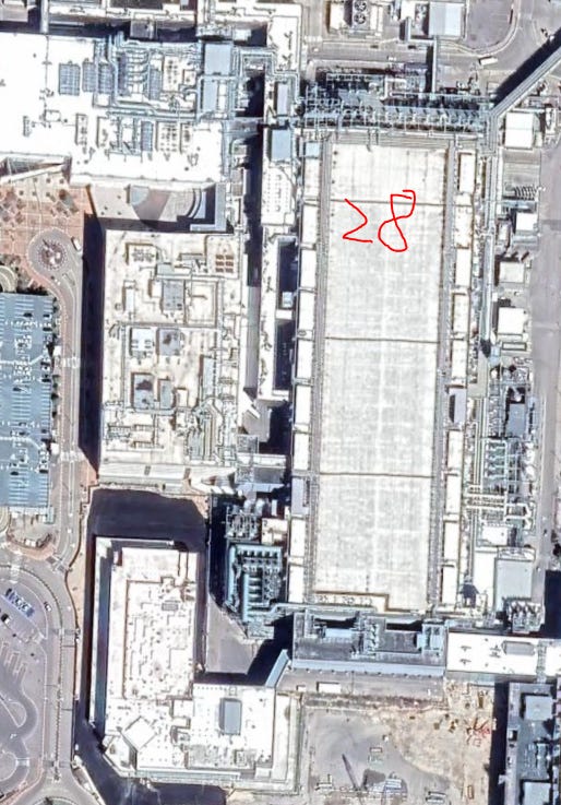
Arizona:
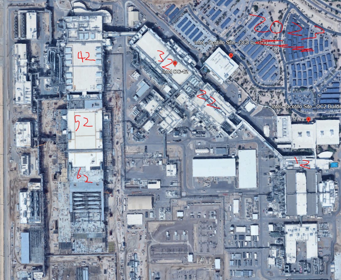
(Fab 52/62 shells are completed, google earth pic is from 2023)
Intel Arizona is Intels single largest site for manufacturing based on its cleanroom capacity. Intel Arizona will be the lead site for 18A volume manufacturing, Arizona is also the home to Intel’s R&D for advanced packaging.
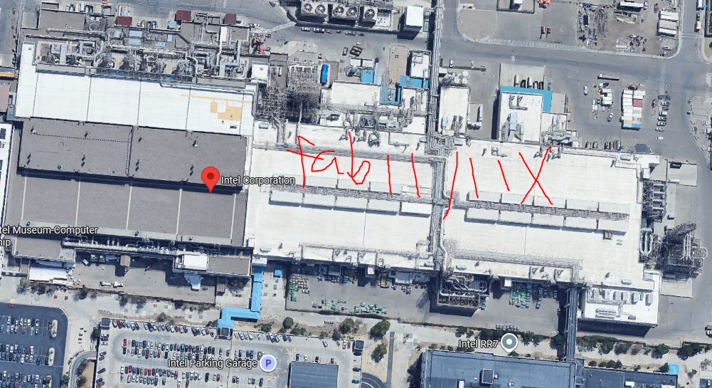
Fab 12
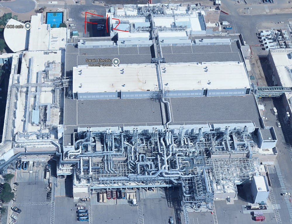
Fab 12 construction started in 1994, and the fab came online as a 200mm wafer fab in 1997 with a cost of $1.3 billion. Fab 12 has a cleanroom size of roughly 140,000 square feet and lacks the vertical clearance to install EUV machines (Some sources point toward 132,000 square feet of cleanroom space). Fab 12 was upgraded to 300mm wafers in 2004 and reopened in 2005. The fab supports Intel 22nm, 14nm, and 10nm production. Fab 12 is currently being repurposed to support the Intel-UMC 12nm node.
Fab 22
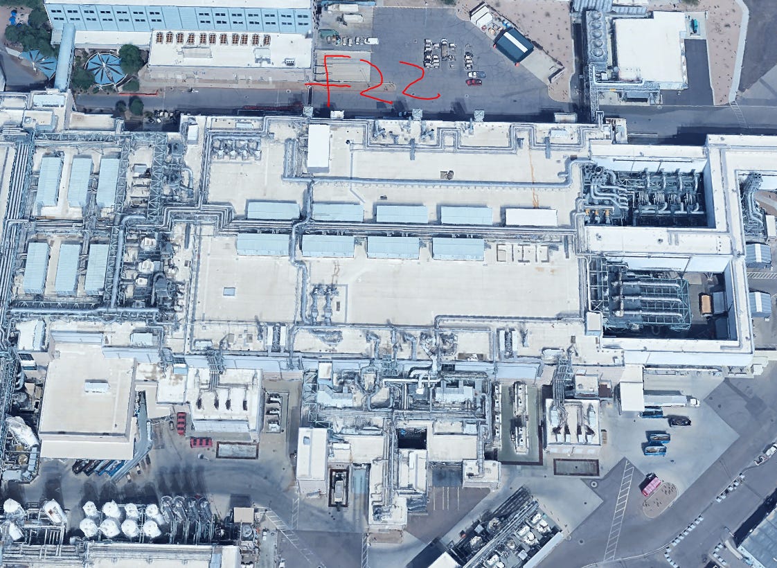
Fab 22 construction started in 2000, and the fab came online just 18 months later at the end of 2001 (Wow, back when the US could build quickly). Fab 22 cost $2 billion and has a cleanroom space of roughly 133,000 square feet. Like Fab 12, it lacks the vertical clearance to install EUV machines (Note that Fab 12 is likely this size as well, despite sources claiming 140,000). Fab 22 supports Intel 22nm, 14nm, and 10nm production. Fab 22 is being repurposed to support the Intel-UMC 12nm node.
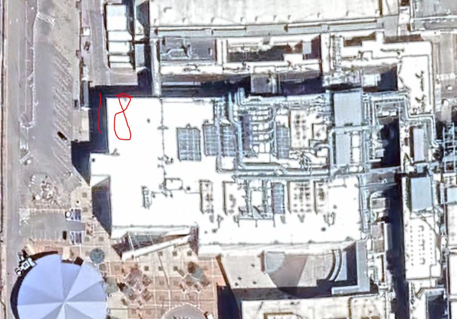
Fab 32
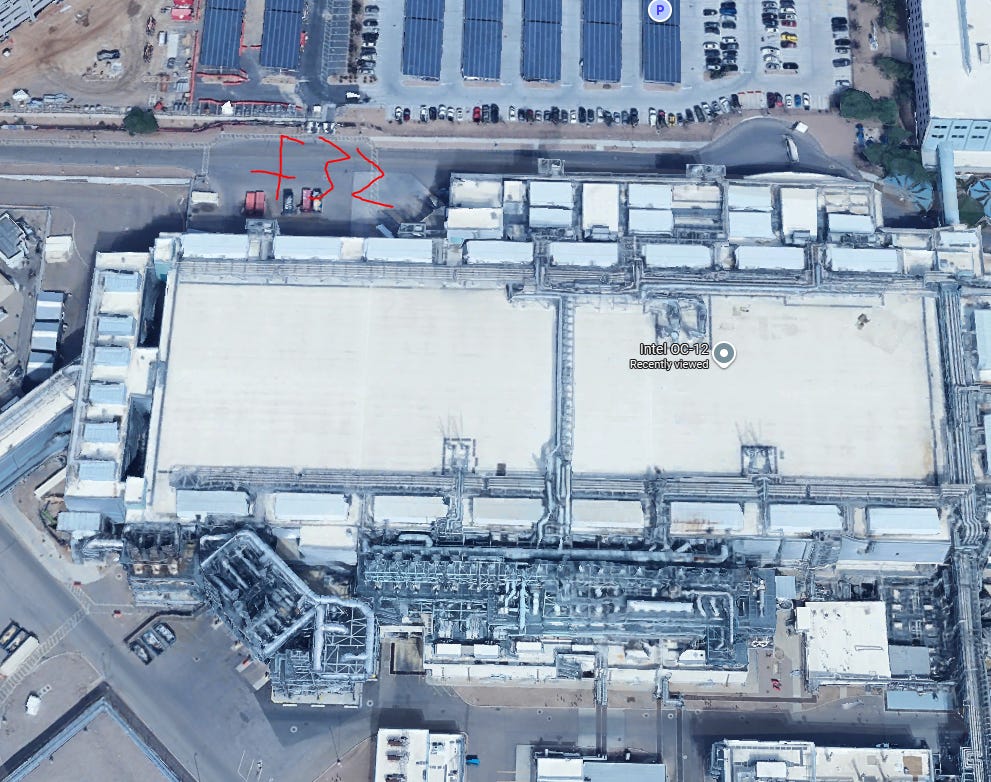
Fab 32 construction started in 2005, and the fab came online in 2007. The facility cost $3 billion. Fab 32 has a cleanroom size of 184,000 square feet and lacks the vertical clearance to install EUV machines. It primarily produces Intel 7. Fab 32 will be repurposed to support the Intel-UMC 12nm node, though hopefully not.
Fab 42
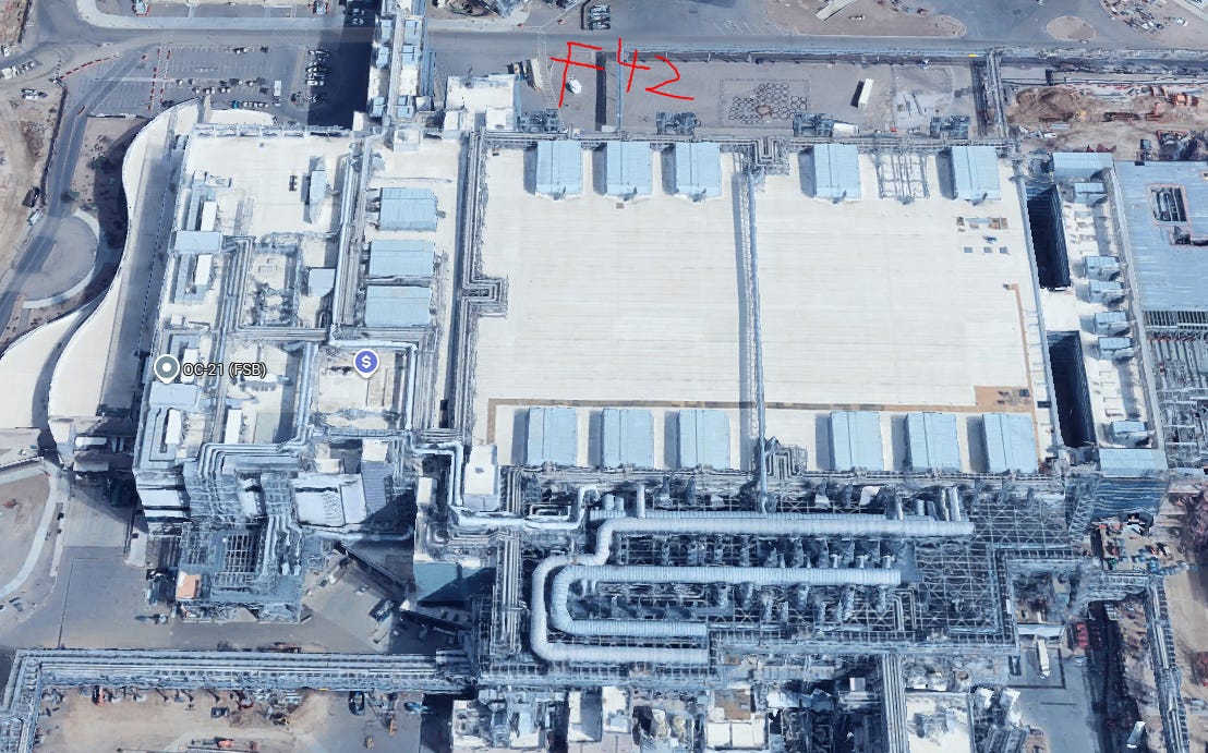
Fab 42 has an interesting history. Construction started in 2011, and it was Intel’s first production fab to meet the vertical clearance requirements capable of installing EUV machines. Fab 42 has 240,000 square feet of cleanroom space. The facility cost $5 billion in 2011 and was intended to be ready for production in 2013, supporting the 14nm generation.
However, subsequent PC demand did not keep growing as expected globally. Purchasing intervals leveled off and a newer, slower growth emerged. Due to these factors, Intel announced in early 2014 that Fab 42 would be mothballed. It was expected that Fab 42 would be used for 10nm, but due to Intel’s incompetent management, 10nm was delayed for years. Then in 2017, Intel announced at the White House that Fab 42 would support Intel 7nm (Intel 4) with a $7 billion investment.
Intel 7nm hit multiple delays, so finally in 2020 Fab 42 became operational producing Intel 10nm (Intel 7). Intel needed this capacity in 2020 due to surging PC demand, but by October 2024, they were swimming in excess capacity and needed the depreciation off their books. How much did the 10nm upgrade cost versus Intel 7nm? Well, Intel’s write down of $3.1 billion in 2024, on a 7 year depreciation schedule, implies $7.23 billion. Not all of it was Intel 7, so we can ballpark $5 billion to $6 billion in tools for this fab.
Since this write down, Intel is running very short on capacity for Intel 7. They could have sold more consumer and data center parts if this capacity had not come out. Was it a mistake? Yes, but it was almost impossible to know they should have doubled down on cheap Intel 7 parts while a decent chunk of the market did not want expensive TSMC N3B CPUs.
After the write down, Intel has begun retooling Fab 42 for 18A. Fab 42 is wholly owned by Intel, so wafers coming out of this fab will have the most dollars going to the bottom line. Intel says the cost for Fab 42, 52, and 62 is $32 billion. Since it states Fab 52 and Fab 62 are $25 billion for 40k WSPM, the Fab 42 upgrade is, you guessed it, $7 billion! Given $25 billion for 40k WSPM across 685,000 square feet, Fab 42 with 240,000 square feet of cleanroom space should be able to do 14k WSPM of Intel 18A.
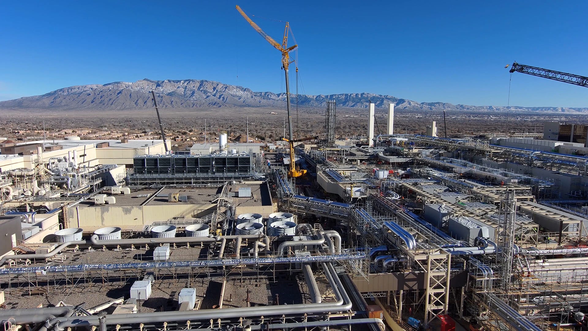
Fab 52 AND Fab 62
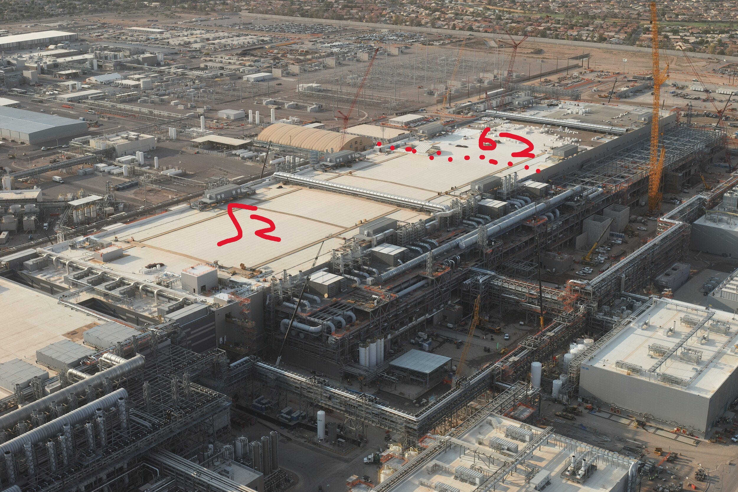
(Whole fab is now done, picture is old)
Fab 52 and Fab 62 were originally called 52.1 and 52.2 because they are really one fab with two modules. Construction started in 2021, and together they have 685,000 square feet of cleanroom space with the vertical clearance for EUV.
The first module, Fab 52, began tool installation roughly a year ago and initiated a dual ramp in both Oregon and Arizona. Intel previously used a “Copy Exactly” strategy where yields in Oregon would stabilize at a high level before the ramp began in HVM fabs.
Intel is no longer doing that. Instead, they are bringing tools in earlier to have two fabs work on yields simultaneously. TSMC employs this strategy, and it is much more effective than Intel’s old method.
Intel has not fully tooled Fab 52. From a CNBC video, we saw four EUV tools installed in the bay, which is capable of holding six. Fab 52 has another bay of six that was not visible, with an unknown number of tools installed. If anyone is doing a tour, let us see the second bay! Fab 52 should be capable of 20k WSPM of 18A.
However, this fab has a caveat unlike previous ones. In 2022, Intel saw that their cash flow was about to tank due to PC demand falling off and a less competitive roadmap thanks to Bob Swan. Consequently, they decided to do a Joint Venture with Brookfield for this fab. Intel has 51% ownership of the profits and puts in 51% of the capital, while Brookfield puts in 49% of the capital. We also have to keep in mind that the US Government has a 25% tax credit for everything related to building and tooling a fab. This goes up to 35% next year, so Intel actually puts in less capital than the 51% ownership.
Regarding the future, John Pitzer has hinted that Fab 62 is currently planned to support 14A. Things could change, but at the moment, that seems to be the plan. Hopefully, over the course of this year, Intel is able to secure enough external 18AP and 18AP-T (backside power SRAM base tiles) orders so we can see Fab 62 tool up quickly for orders in late 2027 into 2028. 18AP-T is likely to be an extremely long life node, and I think it is a mistake to tool Fab 62 for 14A as Intel will need a lot of 18AP-T for AI ASICs.
JUST SAY NO TO 14A!
Oregon:
Intel’s Oregon site is the heart of America’s only leading edge R&D process development site. Intel Oregon has more than 15,000 employees whose job is to keep Moore’s Law alive in the USA.
This site is what makes Intel infinitely more important than any fab from a foreign company. Only three places in the world attempt to stay at the leading edge: Pyeongtaek in South Korea, Hsinchu in Taiwan, and Hillsboro in Oregon. TSMC and Samsung will never move the heart of their R&D to the US. It is of the utmost importance that Hillsboro continues to thrive so we never have to rely on foreign tech transfers.
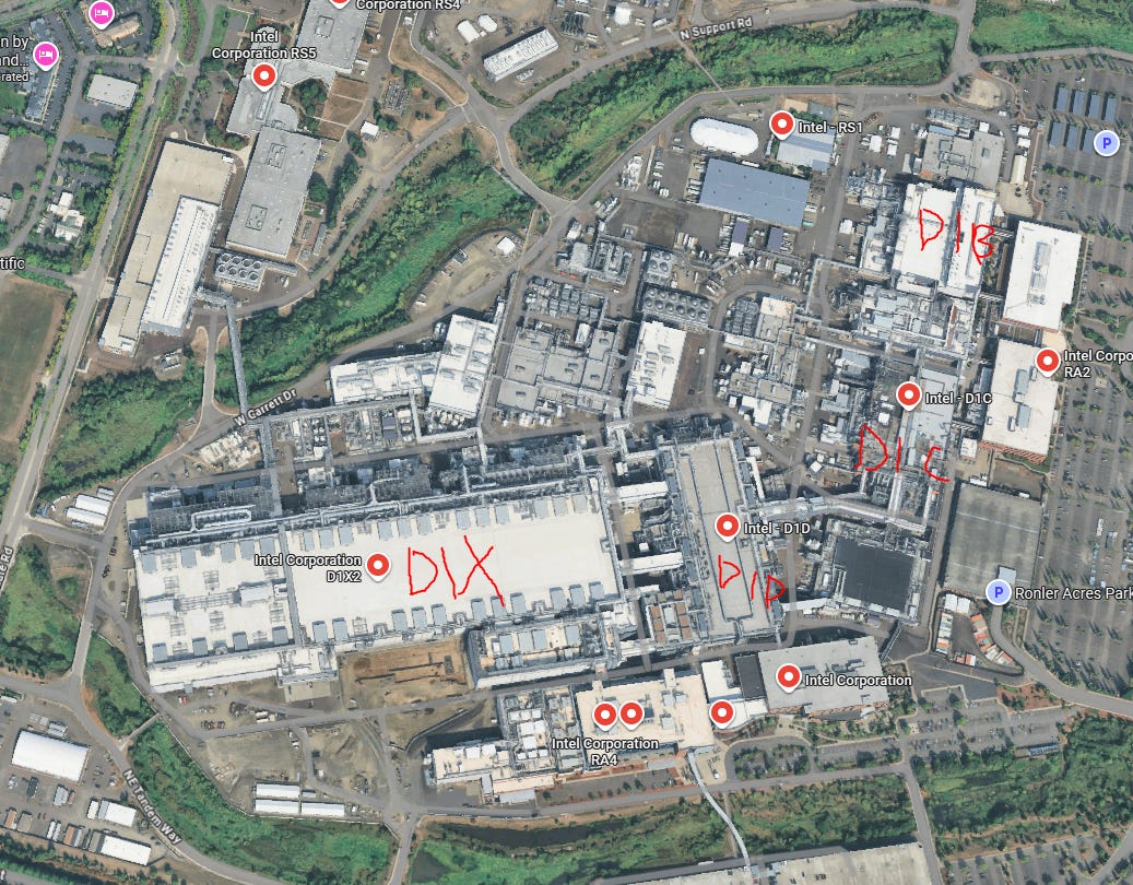
D1B
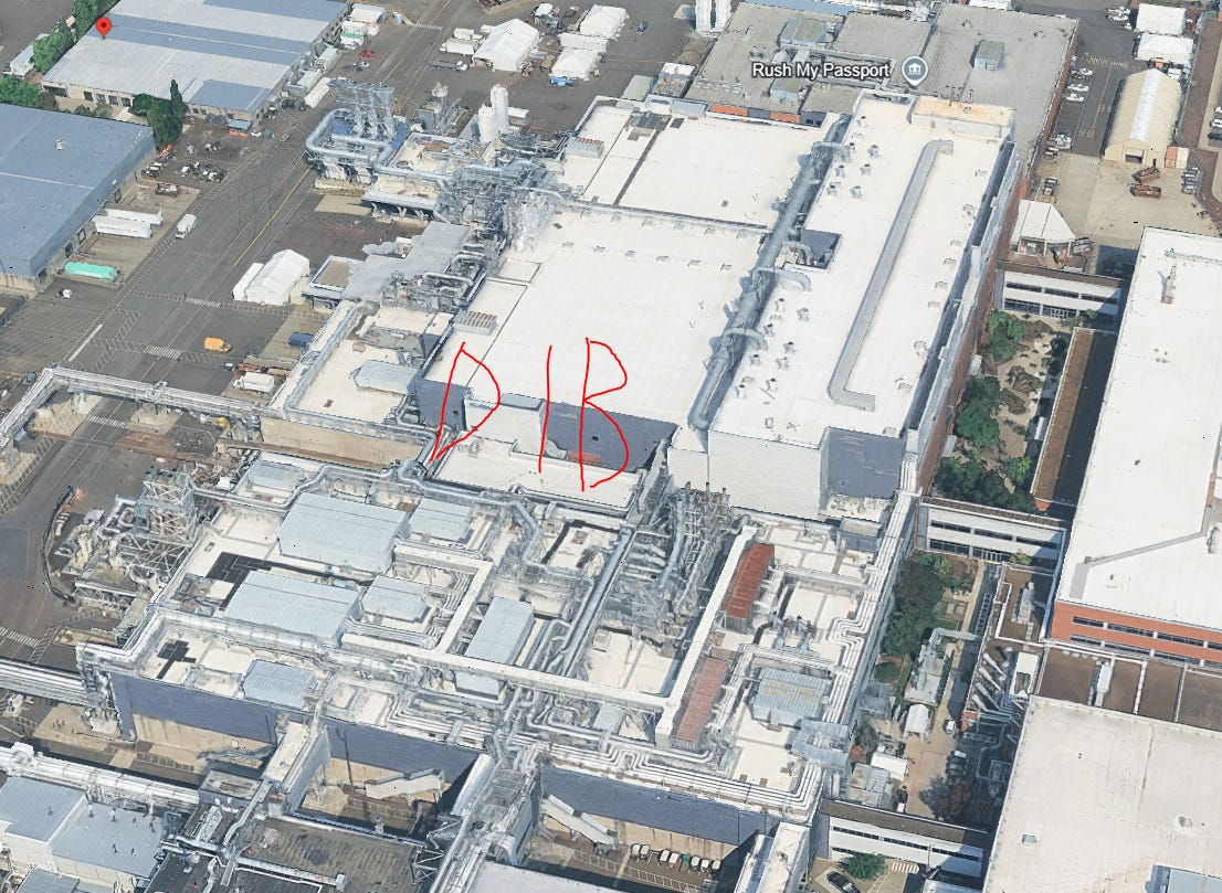
D1B started construction in 1994 and was opened in 1996. It originally had a cleanroom size of 35,000 square feet which was later expanded to 77,000 square feet.
D1C
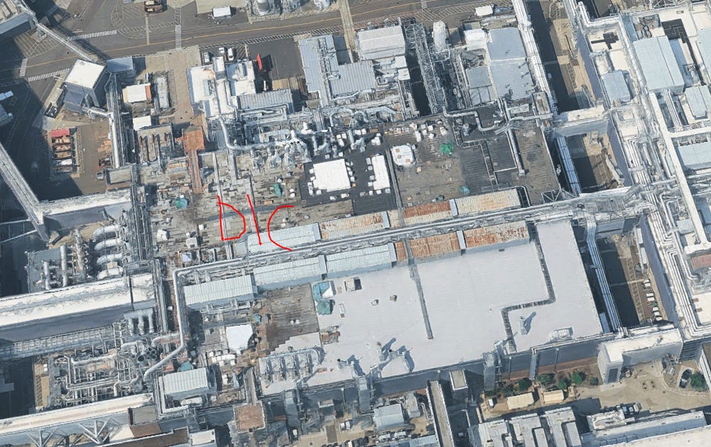
D1C construction started in 1998, and the fab reached volume production by 2001 with a cost of $1.5 billion. It was the world's first 300mm wafer fab, featuring 135,000 square feet of cleanroom space. It was also the world's first facility to utilize FOUP technology and was much more automated than any previous fab.
D1D
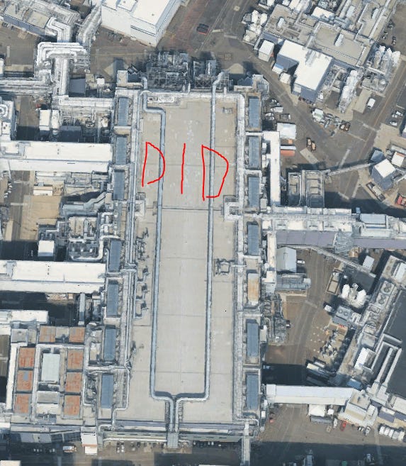
Intel started construction of D1D in 2001, and it reached volume production by 2003. It features 176,000 square feet of cleanroom space and cost $2 billion.
D1X
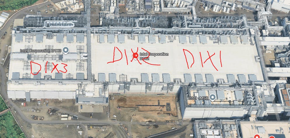
D1X consists of three modules, and it was Intel’s first fab capable of housing EUV tools. It is truly the heart of Intel process node development.
D1X Mod 1 construction started in 2010. It features 240,000 square feet of cleanroom space and cost $3 billion. D1X Mod 1 opened for volume production in 2013.
D1X Mod 2 was announced in 2012 and features 240,000 square feet of cleanroom space with a similar construction cost of roughly $3 billion. It was ready for production in 2015 but was mothballed for cost reasons until 2017.
D1X Mod 3 was announced in 2022 and features 270,000 square feet of cleanroom space and costs near $4 billion. This module recently received a High NA tool. Together, D1X features 750,000 square feet of cleanroom space, all of which is EUV capable.
New Mexico:
Intel New Mexico used to be an R&D hub for Optane (please bring it back). It currently supports manufacturing for Intel's advanced packaging, including bridges and Foveros. It also supports Intel's silicon photonics products. Furthermore, New Mexico is supposed to have a 65nm production line via a collaboration with Tower.
Fab 9
Fab 9 has an interesting history. It was a 200mm fab built in the 1980s that was later merged with Fab 11. The name died, but Intel revived it in 2021 for a new advanced packaging facility in the US. Almost all of Intel's products are packaged here currently. The cost was $3.5 billion. I cannot find any public information about its cleanroom space. However, given D1X Mod 3 has 270,000 square feet of cleanroom space and cost $4 billion, and considering this fab does not need to be EUV capable, it may be around that size.
Fab 11/11x
Fab 11 started life in 1995 as an expansion to Fab 9. The Fab 11 expansion added 45,000 square feet of cleanroom space. The second phase of Fab 11 was announced in 2000 and became called Fab 11X. It added an additional 135,000 square feet of cleanroom space, finishing in 2002 at a cost of $2 billion. Fab 11 likely has north of 200,000 square feet of cleanroom space, given that the original Fab 9 was merged with Fab 11 before the additional expansions.
Intel Ohio:
Please watch Lukateake drone footage for Intel Ohio updates
https://youtu.be/PkZ1g2X_tDE?si=rmB2yhnTXqdVWjQu
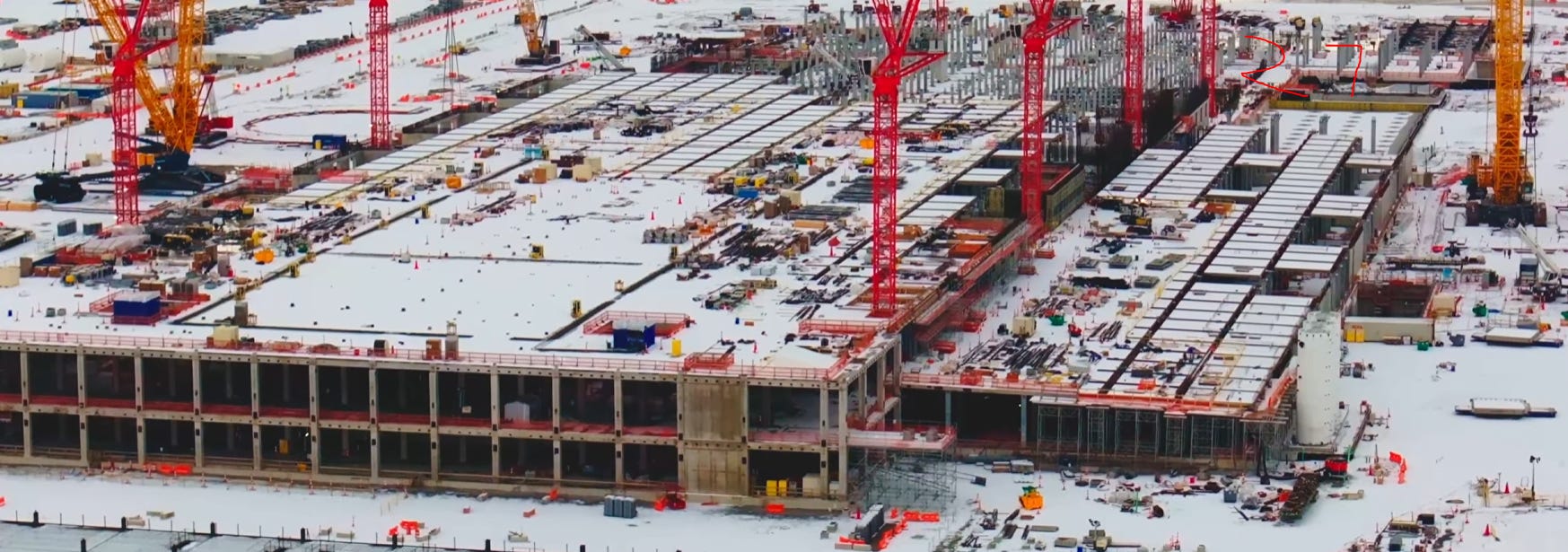
Fab 27 (please rename it Fab 47 for Trump, come on that is a good idea) was announced in 2022 and is currently under construction. Intel Ohio has been delayed repeatedly due to a lack of customers. The project is expected to cost north of $28 billion.
Fab 27 is the same size as Fab 52, Fab 62, and Fab 38, featuring 685,000 square feet of cleanroom space. The current opening date is expected to be 2032. However, Intel has repeatedly said it can accelerate Fab 27 to be ready for 14A. This would likely mean 2028 given the fab’s progress.
Sign up now!

We need to finish this site and get the three remaining fabs started for the Intel 10A node in 2030. The US government seems ready to help get these shells started so we have capacity if something happens to Taiwan. We need a lot more, but it is something.
Intel Ireland
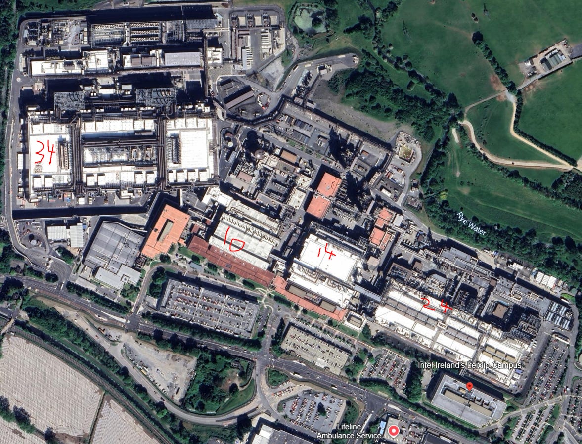
Intel came to Ireland in 1989, and today the site has Europe’s most advanced semiconductor fab. Intel Ireland has produced every Intel technology up until Intel 18A. Until Fab 28 in Israel came online, Intel Ireland represented 25% of Intel's production, with 75% remaining in the United States.
Fab 10
Fab 10 construction started in 1990. The facility opened in 1993 and cost $300 million. Fab 10 has 70,000 square feet of cleanroom space. It supported 14nm production in Ireland and today supports Intel’s 16nm node. Fab 10 is also being used to increase Intel 3 production in Fab 34 by utilizing its existing tools.
Fab 14
Fab 14 construction started in 1995. It opened in 1998 and cost $1.3 billion. Fab 14 has 90,000 square feet of cleanroom space. The facility supported 14nm production in Ireland and today supports Intel’s 16nm node. Fab 14 is also being used to increase Intel 3 production in Fab 34 by utilizing its existing tools.
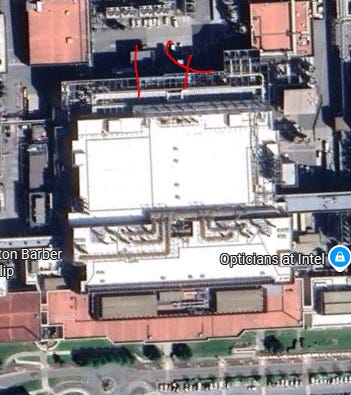
Fab 24
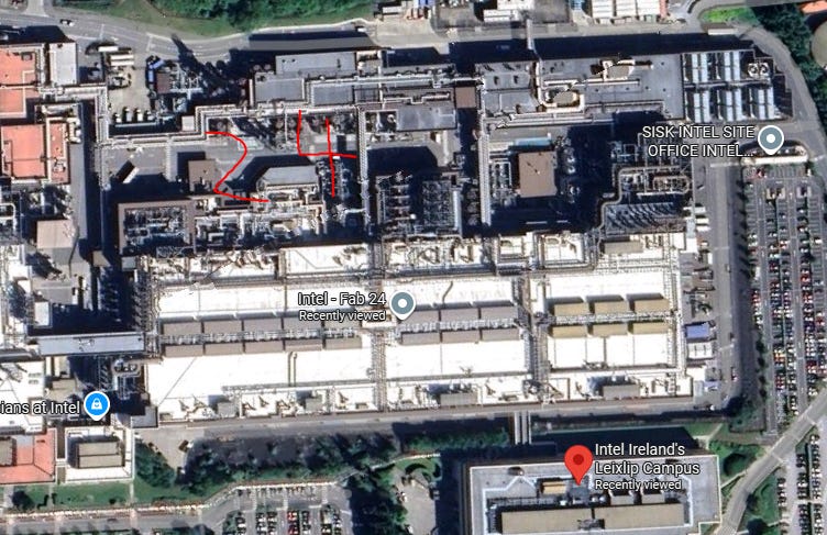
Fab 24 construction started in 2000. It opened in 2004 with a one year delay due to the dotcom bubble. Fab 24 cost $2 billion and has 135,000 square feet of cleanroom space. In 2004, Intel also announced a second module known as Fab 24 Module 2. The second module added 60,000 square feet of cleanroom space for a total of 195,000 square feet. It cost another $2 billion as process node costs began to rise. Fab 24 supports 14nm production, which is dwindling, and Intel 16. It is primarily used to support Intel 3 production in Fab 34.
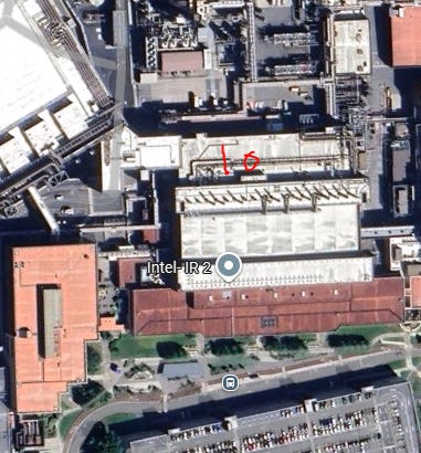
Fab 34
Intel Ireland started construction in 2019, and the facility began volume production in 2023 with a cost of $19 billion. Intel Ireland has two modules. Each module is 215,000 square feet, for a total of 430,000 square feet of cleanroom space.
Due to Intel’s cash burn, Intel made the unfortunate decision to sell 49% of Fab 34 for $11 billion to Apollo. Intel would have been better off getting government financing or raising money from potential customers. But that sadly did not happen in 2024. The planned WSPM for Fab 34 is likely 40k WSPM currently, based on the Foundry Day 2024 chart.
Intel Israel:
Intel came to Israel in 1974 when they opened a design center in Haifa. Intel did not have a manufacturing presence in Israel until 1985 when they opened Fab 8 in Jerusalem. Today, Intel’s manufacturing home is in Kiryat Gat. Intel Israel regularly hits the highest yields of any site and could be where the first 14A wafers are started for volume production.
Fab 18
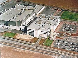
Fab 18 started construction in 1996 and opened in 1999. The fab cost $1.6 billion and featured a 96,878 square foot cleanroom, but it was a 200mm wafer fab for NAND flash. Intel later sold it to Micron before Micron Israel underwent restructuring and decided that Intel should take over the facility. Intel later upgraded it in 2014 to support Fab 28 22nm production. Fab 18 continues to support Fab 28 10nm production.
Fab 28
Intel announced Fab 28 in 2005, and the facility opened in 2008 with a cost of $3.5 billion. Fab 28 features 200,000 square feet of cleanroom space. It is Intel’s main fab supporting 10nm following the Fab 42 conversion to 18A.
Fab 38
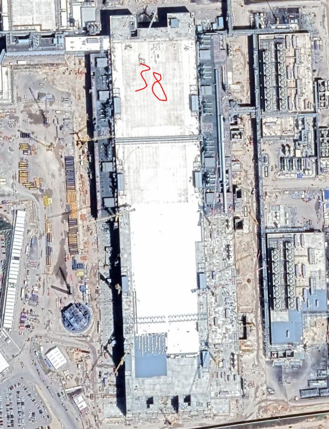
(March 2025)
Intel announced Fab 38 in 2022. The facility is currently under construction and is expected to cost more than $25 billion. Fab 38 was delayed in 2024, but construction has continued to finish the shell at a slower pace. Fab 38 is the same size as Fab 52 and Fab 62, featuring 685,000 square feet of cleanroom space. Fab 38 is likely to support the Intel 14A ramp.
Intel Malaysia
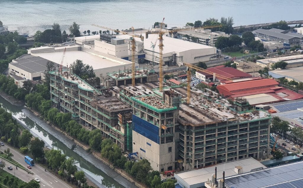
(Older picture, the shell is almost done)
Project Pelican is Intel’s $7 billion advanced packaging site featuring 710,000 square feet of cleanroom space across two levels. Project Pelican will be Intel’s largest advanced packaging site and is slightly smaller than TSMC AP8, which has a 1 million square foot cleanroom.
TSMC AP8 itself will double TSMC advanced packaging capacity. So we can truly see how much capacity Intel has to do advanced packaging. Intel’s EMIB solution is also more efficient given it does not need to waste silicon on wafers. Instead, it is a silicon bridge.
Summary of Cleanroom Space per Site
Arizona
930,000 square feet EUV
Roughly 456,000 square feet Non-EUV
Oregon
750,000 square feet EUV
Roughly 388,000 square feet Non-EUV
New Mexico
Guesstimate of 470,000 square feet Non-EUV (Advanced Packaging, used to do Optane)
Ohio
685,000 square feet EUV (Expected 2028 to 2029)
Ireland
430,000 square feet EUV
Roughly 355,000 square feet Non-EUV
Israel
685,000 square feet EUV (Expected 2028)
Roughly 300,000 square feet Non-EUV
Malaysia
710,000 square feet Non-EUV (Advanced Packaging)
Total Cleanroom Space Ready by End of 2028
2.3 million square feet EUV Volume
750,000 square feet EUV R&D
1.5 million square feet Non-EUV Volume
Roughly 1.18 million square feet of Advanced Packaging
Intel WSPM Model
There are some key assumptions that I am using that could break my model if proven untrue. First is this infographic from Intel in 2024. Ignore the SemiAnalysis watermark as they did not make it.

Intel states roughly $25 billion per 10,000 WSPW (40,000 WSPM) for Low-NA. Intel Fab 52 and Fab 62 were initially $20 billion, but inflation took it to $25 billion. This tells us Fab 52 and Fab 62 are 40,000 WSPM 18A fabs.
Second is a bar chart from Intel.

A couple of things to keep in mind are that WSPW (I am going to use WSPM) per bar are not normalized for a single node. I am also not going to count Oregon initial HVM in my numbers, considering this is short-term production that is run, deramped, and prepared for the next node.
EUV Ireland is Intel 3, while EUV Arizona is 18A. We can see Intel Ohio, which has no other supporting fabs, is the same height as the EUV Israel bar. This tells us both Ohio and Israel are just numbers from Fab 38 and Fab 27. Given the infographic above, neither of these bar charts can be above 40,000 WSPM.
If we take this as our understanding, then we can work backwards to find Intel’s current maximum WSPM. There is also a neat trick given we know the Non-EUV cleanroom space of Israel (slightly above 300,000 square feet), which is exclusively doing 10nm. We can then look even further back given I have all the cleanroom spaces for Intel’s production fabs. We can calculate what I am calling the ‘10nm equivalent,’ aka Intel’s WSPM in 2022 if all their fabs were doing 10nm.
Keep in mind, Ireland and some parts of Arizona were doing 14nm, but there is no easy comp for that. That would have increased Intel’s WSPM given 14nm uses fewer steps.
I invite you to open Windows Designer and move around lines to calculate ratios and give feedback on what you think.
Intel WSPM Math: Current Plan
Arizona EUV
Fab 52 and Fab 62 comprise 685,000 square feet of cleanroom space. With the addition of Fab 42, which has 245,000 square feet, the total Arizona EUV capable space is 930,000 square feet.
If 685,000 square feet of cleanroom represents 40,000 WSPM of 18A, we can estimate the capacity of Fab 42. The ratio of 245,000 to 685,000 is 0.35766. Multiplying this by 40,000 gives us 14,300 WSPM from Fab 42. This would yield a total of 54,300 WSPM for the EUV Arizona bar. Intel is using half of this, given the “2X” figure on top, so there are 27,100 WSPM of 18A planned. I am going to address all Non-EUV WSPM below this.
27,100 WSPM 18A TODAY
54,300 WSPM MAX
Ireland EUV
Given the ratio of the top of the Arizona bar is 54,000 WSPM, the Intel Ireland EUV bar implies a maximum of roughly 65,000 WSPM of Intel 3, with current planned production of roughly 40,000 WSPM.
Now, some of you are going, “Hey, how is Intel getting 65,000 WSPM out of Ireland, which is a 420,000 square foot fab?”
Part of the reason is that a less dense process like Intel 3 requires fewer steps. This means the WSPM is higher. But Intel is also boosting EUV wafer starts using Non-EUV cleanroom space. Intel Ireland’s Non-EUV cleanroom space is roughly 355,000 square feet. Yet Ireland, which is supposed to only support Intel 16/14nm, has a very low WSPM in the chart.
Considering that Non-EUV Arizona has roughly 456,000 square feet of cleanroom space, the bar chart for Ireland should show 54,000 WSPM of Intel 7 and Intel 12. Well taking a look its much, much, smaller. This is because Intel is using tools in those fabs to lift Intel 3 production, either with existing tools or even some new ones.
40,000 WSPM TODAY
Roughly 65,000 WSPM MAX
Israel/Ohio EUV
Neither the Israel nor the Ohio EUV fabs are currently in production. However, doing some ratio analysis on the chart implies that both of these bars seem a little too short to be 40,000 WSPM. This makes sense given that the Israel Non-EUV and Ireland EUV bars are about the same height.
Given that both of these fabs are 14A, it follows that they would fall short of 40,000 WSPM. 14A uses more steps, the cleanroom space is the same as in the 18A fab, and tool productivity is unlikely to make up for it completely. Based on the ratios, it seems to me that Fab 38 and Fab 27 are roughly 36,000 WSPM for 14A.
36,000 WSPM Ohio 14A (2028)
36,000 WSPM Israel 14A (2028)
Arizona Non-EUV
Now here comes a bit of a rub. Intel does not seem to be yet using the Non-EUV space to juice wafer starts of 18A. But given Arizona has 456,000 square feet of Non-EUV space, shouldn’t its WSPM be higher if it is doing Intel 12nm and Intel 7? The answer is yes.
If Arizona were using all of its cleanroom space for Intel 7, wafer starts would be roughly 60,000, which is a tad higher than 54,300. But Intel 12 uses fewer steps, so volume would be higher. I suspect Intel likely reserved some cleanroom space for R&D wafers of Intel 12.
Ultimately, how many Intel 12 wafers is Intel going to sell?
It is nice to use Intel 12 for some old equipment. But if foundry demand really picks up, Intel is best off doing small Intel 12 volume and enough Intel 7 volume to stay in the Altera contract. Maybe Fab 12 is for Intel 12 and 7, while Fab 22 and 32 are used for 18A.
27,100 WSPM TODAY
Roughly 54,300 WSPM MAX (Intel 7, Intel 12)
Israel Non-EUV
Israel Non-EUV space is dedicated to doing Intel 7 and 10nm currently at roughly 40,000 WSPM. There is excess demand for these products this year and likely into the next. The main issue is what to do in 2028.
Intel will have long-run products on Intel 7 for embedded and telco applications. There was also a rumor that Intel is using SF8 next year for motherboard chipsets. Maybe come 2028, Intel will use Israel 7nm for chipsets, so production continues.
People have also discussed maybe an Intel-UMC 6nm node. I kind of doubt it given the cost decisions made with Intel 7nm and the redesigns needed. I think it is likely Intel continues a minimum level of 7nm wafers and decides to juice Intel 14A for Fab 38.
Roughly 40,000 WSPM Intel 7 TODAY
Ireland Non-EUV
Ireland’s Non-EUV space is primarily doing Intel 22nm, 14nm, and Intel 16. Intel must continue these nodes for legacy products and some small volume Intel 16 clients. The bar chart implies something like 16,000 WSPM for these with an upside to roughly 24,000 WSPM.
Roughly 16,000 WSPM (Intel 14nm, Intel 22nm, Intel 16) TODAY
Roughly 24,000 WSPM MAX
__________________________________________________________
I believe fully that 18AP-T in Arizona is going to be a massive node, and Intel really needs to max out production. Intel will be the first to have a base die that has backside power, and no other foundry will have a cheap backside power base die because they never relaxed the pitches. If you want SRAM caches, nothing will beat 18AP-T. Intel shouldn’t even make other products using 18A; they will be sold out of 18AP-T.
Now, this is what Intel should do, and I have heard some hints that they might pursue this path.
So what if Intel ditches some of the older node production to max out 18A and 14A?
Lip-Bu, Fab 62 should not be 14A!
If Intel ditches Fab 32 and Fab 22 from doing Intel 7 and most of Intel 12, we can get a total cleanroom space of roughly 1.26 million square feet, with only Fab 12 doing Intel 7 and Intel 12. That pushes up 18A WSPM by another 26,600. That would mean Arizona could do roughly 81,000 WSPM of 18A instead of 54,300. Who wants to sell a $7,000 wafer when you are supporting a ~$23,000 18A wafer?
Whatever Intel is considering for Intel 7 in Israel, keep it to a minimum. Let’s buy Samsung 8nm, who cares?
Let’s consider Intel keeping roughly 100,000 square feet of cleanroom space for Intel 7 (legacy products must be supported). Then have 200,000 square feet of cleanroom space to support 14A in Fab 38. We go from 36,000 WSPM of 14A to 46,000 WSPM of 14A.
These moves mean that in 2028 (really into 2029), Intel Foundry will do the following or be close to ramping to this capacity:
81,000 WSPM of 18A
82,000 WSPM of 14A (Combining Ohio and the boosted Israel capacity)
65,000 WSPM of Intel 3
Minimum of 31,000 WSPM Intel 7 equivalent (some of this could be Intel 12, so actual WSPM would be higher)
24,000 WSPM of Intel 16
Oregon for a short time, might increase 14A capacity by roughly 20,000 WSPM. But it will deramp for 10A support. I am not sure how you want to account for this.
Total Capacity:
163,000 WSPM of Leading Edge
65,000 WSPM Trailing Edge
55,000 WSPM Legacy
__________________________________________________________
Now, for fun, let’s go back in time. We can do some back-of-the-envelope math to see how much “10nm equivalent” capacity Intel had by the end of 2021. This was Intel at “Peak IDM,” before the TSMC outsourcing of N3B and N6. It was also before desktop volume went down 30%, notebook volume fell 20%, and server volume fell by 50%.
Given we know 300,000 square feet of cleanroom space represents 40,000 WSPM of Intel 7, we can see what Intel was doing at its peak.
Arizona
Non-EUV Space: 456,000 + 245,000 (Fab 42) = 701,000 square feet.
This translates to 93,400 WSPM.
Israel
Non-EUV Space: 300,000 square feet.
This translates to 40,000 WSPM.
Ireland
Ireland never did Intel 10nm/Intel 7; it was 14nm. However, assuming the “10nm equivalent” based on its 355,000 square feet of cleanroom space:
This translates to 47,300 WSPM.
New Mexico and Malaysia
N/A
Total That means at the end of 2021, Intel was doing—drum roll please—180,000 WSPM of Intel 7 equivalent (likely over 200,000 WSPM when the less steps required of 14nm is accounted for).
__________________________________________________________
Intel’s planned capacity, at least in early 2025 (remember 18A had not ramped yet), was roughly:
20,000 WSPM N3B
30,000 WSPM Intel 3 (Guessing here, hard to know to be honest, Intel 3 ramped through the year)
67,000 WSPM Intel 7
16,000 WSPM 14nm/22nm
15,000 WSPM N6 (Maybe? I do not know)
Total: Roughly 148,000 WSPM
__________________________________________________________
Intel will have some N2P orders for 2026, 2027, and 2028. Keep that in mind for modeling.
__________________________________________________________
Also anyone who says Intel doesn’t run 24/7, 7 days a week. You are an idiot
I hope you enjoyed this article! It took me forever to research and write. Below are my sources
__________________________________________________________
https://newsroom.intel.com/intel-foundry/ifs-manufacturing-news-2024 (intel umc)
https://www.intel.com/pressroom/archive/releases/2005/20051102corp.htm (fab 12 reopen)
https://sst.semiconductor-digest.com/1995/01/intel-expansions-endorse-class-1-ballrooms/ (fab 12 cleanroom space)
https://www.intel.com/pressroom/archive/releases/2000/cn012500.htm (Fab 22)
https://www.eetimes.com/intel-completes-0-13-micron-wafer-fab-in-chandler/ (fab 22)
https://www.eetimes.com/intel-to-build-first-300-mm-fab-in-chandler-az/ (fab 22)
https://www.intel.com/pressroom/kits/manufacturing/Fab32/AZFactsheet_FNL.pdf (fab 32)
https://www.oregonlive.com/silicon-forest/2014/01/intel_delays_opening_new_arizo.html (fab 42)
https://www.techpowerup.com/273064/intels-10-nm-geared-fab-42-enters-operational-status (fab 42)
https://www.legitreviews.com/intel-finshed-5-2-billion-fab-42-arizona-last-year-remains-empty_133946 (same sizes?)
NEW MEXICO INFO
https://sst.semiconductor-digest.com/1995/01/intel-expansions-endorse-class-1-ballrooms/
https://www.intel.com/pressroom/archive/releases/2005/20051102corp.htm (IRELAND NEW MEXICO)
https://www.eetimes.com/intel-opens-first-high-volume-300-mm-fab/
https://www.deseret.com/2002/11/4/19686780/2-billion-addition-opens-at-new-mexico-intel-plant/
Intel 1 million wafers
WAFER
https://newsletter.semianalysis.com/p/is-intel-back-foundry-and-product/comments
OREGON:
https://djcoregon.com/news/2002/10/28/intel8217s-ronler-acres-projects-give-corridor-boost/
https://www.intel.com/pressroom/archive/releases/2001/20010402corp.htm
https://www.oregonlive.com/silicon-forest/2012/10/intel_makes_a_bet_on_oregon_an.html
https://www.intel.com/pressroom/archive/releases/2003/20031124tech.htm
Ohio
https://newsroom.intel.com/press-kit/intel-invests-ohio
Ireland
https://www.intel.com/pressroom/archive/releases/1998/AW051198.HTM
https://www.intel.com/pressroom/archive/releases/2004/20040519corp.htm
Israel
https://siteselection.com/ssinsider/bbdeal/bd050801.htm
https://semiengineering.com/10nm-fab-watch/
https://www.intel.com/pressroom/archive/releases/2005/20051201corp.htm
Bro you’re goated.
Thanks for the sources, you’re literally the first one I’ve seen who referenced any relative figures of the process steps for the various nodes. I’ve occasionally searched for these details and rarely found anything that wasn’t vague on specific details like it.